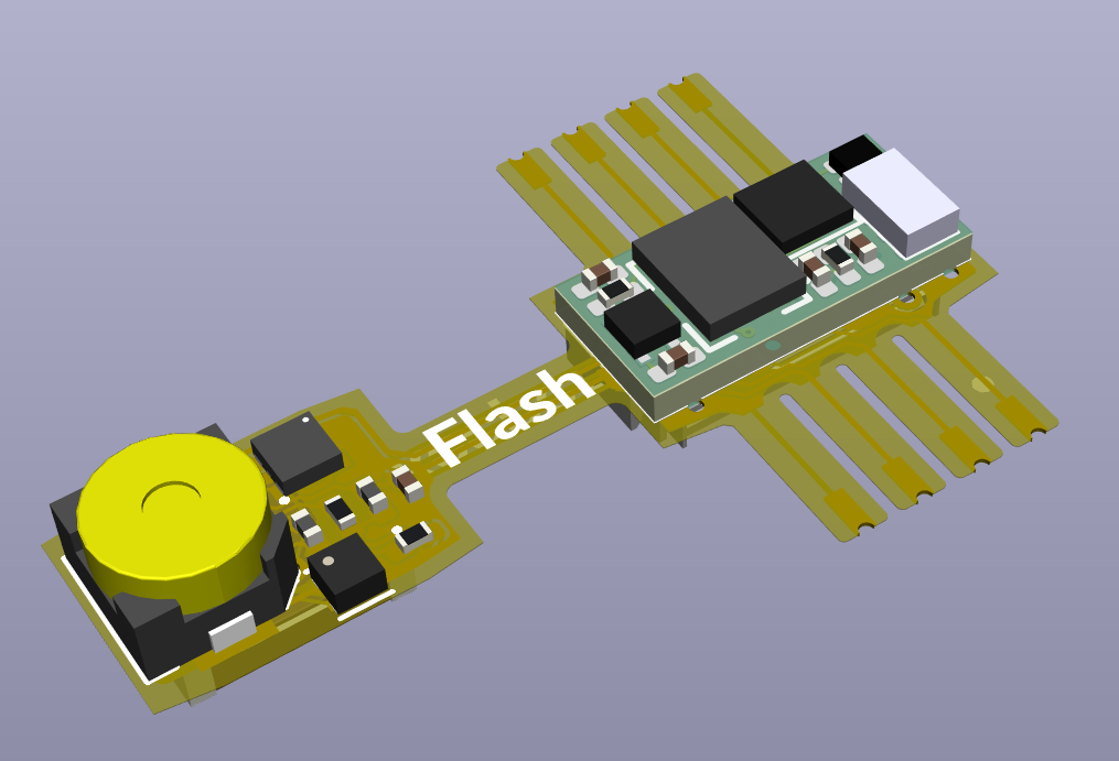
 The Flashkeeper SoM (top), attached to its removable breakout tab with a standard 2.54mm pin header
Introduction
The Flashkeeper FPGA module is special variant of the Flashkeeper chip adapter, designed to interface your SPI flash chip with a specialized Flashkeeper system-on-module (SoM) based on a Lattice iCE40UP5K FPGA. The Flashkeeper FPGA module is a general-purpose computer, under full, RTL-level user control, and designed for a wide range of security, development, and flash device management tasks. In addition to its RISC-V soft core and the hardware reconfigurability afforded by any FPGA, it also features 4 Mbit of NOR flash, 128 kB of main SRAM, one-time programmable NVCM, flexible SPI, UART, and I2C peripherals, a software-controllable buzzer for alerts and acoustic communications, an integrated real-time clock with battery and crystal, and onboard power regulation and filtering for all required voltage rails, including battery charging, from the single power rail on the host flash chip package.
Table of Contents
System Compatibility
The Flashkeeper FPGA module is designed for use on most standard 8-pin NOR flash packages, including most SOIC-8 and WSON-8 variants. The module body, excluding its attachment legs, measures 4.7 x 7.5 mm, and the entire module, when fully folded, stands 6.0mm above the surface of the host flash chip, including its “tail” section (which contains the battery, buzzer, and associated components). In many systems, it can be installed in this folded configuration, with a footprint only negligibly larger than the flash chip itself. Unfolded, it requires only 2.6mm of vertical space above the flash chip, allowing the tail to sit beside the host flash chip.
The folded configuration is recommended for:
- Nearly all desktop and server platforms
- Laptops with sufficient space between motherboard and chassis
- Open-air usage (SBCs, development boards, bench testing, etc)
The unfolded configuration is recommended for:
- Small-form-factor desktop systems with back-mounted SPI flash chips
- Most laptops - fit checks have been performed on various Lenovo ThinkPad X-series (including X220, X230, X140e)
- Systems where the debug ribbon cable is to remain easily-removable (for external flashing, wired verification, development, etc)
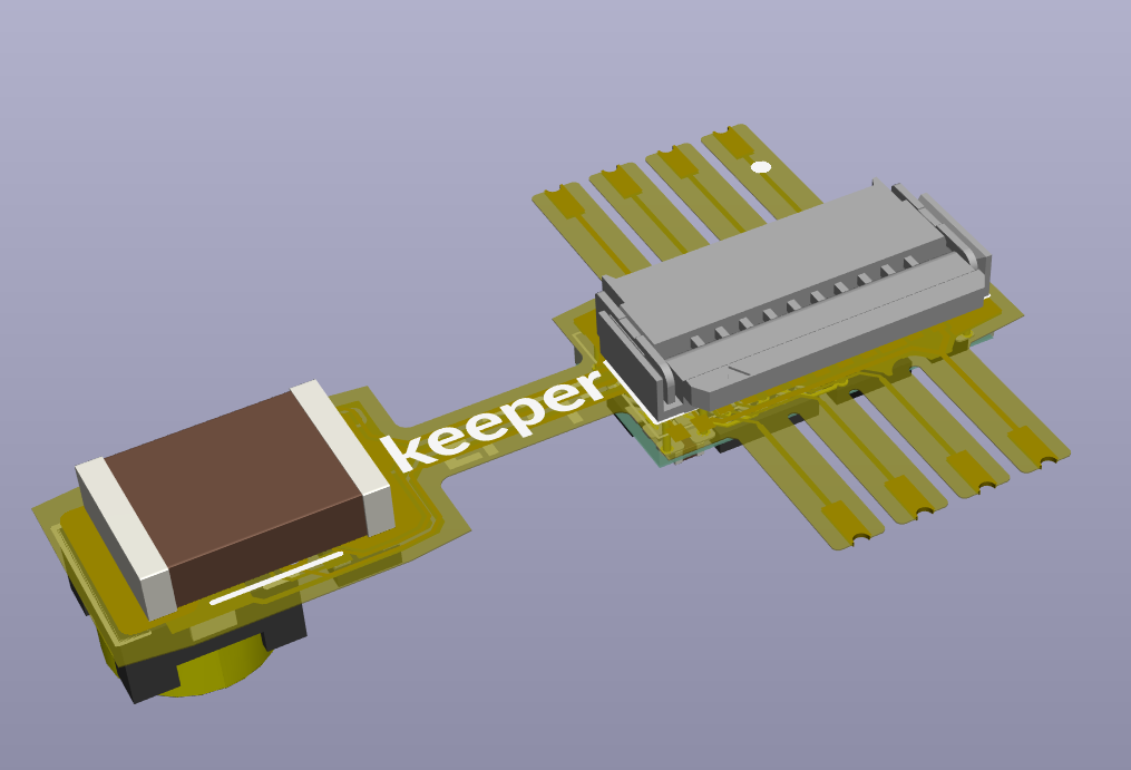 The tail section (left) can be folded over the chip adapter body (right), or can be laid to the side, depending on chassis or board obstructions
The Flashkeeper FPGA draws approximately 9 mA while running, and can be installed with negligible power or thermal impact in virtually any computing device with a SOIC or WSON flash chip - for comparison, many SPI flash chips themselves can consume up to 25 mA while being erased and programmed during a firmware update. All systems we have evaluated for this have had more-than-sufficient current for the module available at the flash package.
The FPGA is only powered when the host SPI flash is, and should not meaningfully contribute to system battery drain in storage. When the host is powered on, Flashkeeper’s real-time clock battery is trickle-charged by a dedicated low-power charging circuit. In order keep the RTC battery charged, host systems should be powered on for at least 2-3 hours per month if Flashkeeper’s real-time clock is required. A diode prevents the RTC battery from discharging into the rest of the SoM, or into the host, when host power is unavailable.
On systems using 1.8V SPI flash, the module is able to generate most of its voltages from 1.8V, but the FPGA itself requires a 2.5-3.3V rail for its internal oscillator and one-time programmable memory. Even on systems with 1.8V flash, 3.3V power is usually available nearby on the motherboard and can be relatively easily wired to the module during installation - a solder jumper and designated pad on the module are provided for this use.