Hardware Architecture
Flashkeeper’s hardware is a modular system, able to be configured for a variety of SPI flash chip security, debugging, and management tasks. Depending on their goals, most users will not need to use every part of the system. This page lists and describes the components of the Flashkeeper system, as well as the major electronic components selected for use in them, and describes some practical combinations of different Flashkeeper components. Much of this document describes “feasibility and selection” research completed before work on Flashkeeper hardware in earnest had begun - as such, it may refer to work already performed (i.e. design of various chip adapters) in the future tense.
Table of contents
Components
Chip Adapter
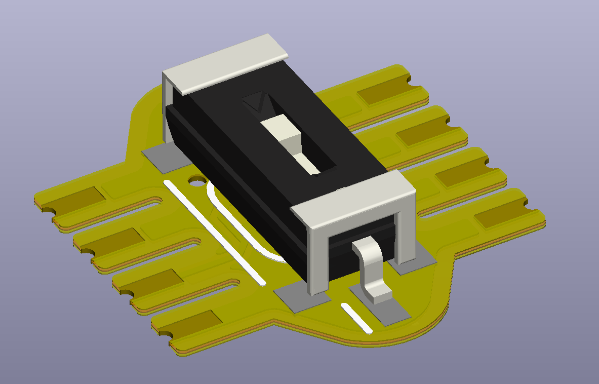
A small flex PCB which installs semi-permanently on top of an SPI flash chip. Provides control over write protection, and a breakout of the SPI bus to external devices. A flash adapter can be:
- Soldered or Solderless
- SOIC-8, WSON-8, SOIC-16, or DIP (SOIC-8 and WSON-8 are the priorities at this time, due to being the most common types)
- WP-only (providing only a switch or a jumper for write-protect control) or Breakout (with a ZIF socket, for all other uses)
As the chip adapter is electrically very simple, across all chip adapter variants, only a handful of components need to be selected:
- DIP switch for WP variants: Nidec CVS-01TB (seemingly the smallest, lowest-profile single DIP switch available)
- Spring-loaded contact for solderless variants: Harwin P70-7000045 (a rare example of a low-profile spring-loaded contact small enough to fit in a 1.27mm pitch)
- Connector for Breakout variants: TBD
Flex Cable
A simple straight-through flex cable which runs from Breakout variants of the chip adapter to other devices, inside or outside the chassis. Connectors should be selected such that commercially-available cables can be used.
External Breakout Board
A board intended for use outside the system, connected to the breakout cable. Useful to connect your SPI flash chip to to devices including:
- External flash programmers (e.g. CH341a), for conventional flashing/unbricking
- Development hardware such as logic analyzers or external (i.e. not the Flashkeeper FPGA Board) FPGA hardware
- The External Flash Emulator
It also allows an alternate use of the flex able, interfacing with the Flashkeeper FPGA board, as opposed to the Chip Adapter. In this role, it can be used as a USB interface board for the FPGA board, for FPGA development and authenticated reprogramming.
External Flash Emulator
The External Flash Emulator is a development tool intended to be connected to the breakout Chip Adapter via the flex cable. It runs SPIspy and has enough memory to fully emulate the SPI flash chip, and is intended primarily as a development/diagnostic tool.
Flashkeeper FPGA Board
The Flashkeeper FPGA is a (very) small board using the Lattice iCE40UP5K, to be installed inside the system. It provides authenticated external reprogramming (via the breakout board), and can also be used to verify flash contents in-situ (similar to the functionality of Intel’s Boot Guard, but under user control). Major components of the FPGA board include:
- FPGA: Lattice iCE40UP5K-UWG30
- 1.2V Voltage Regulator: TI TPS7A2012PYCJR
- 1.8V Voltage Regulator: onsemi NCP110AFCT180T2G
- FPGA Flash Chip (firmware only - gateware burned to NVCM): BYTe BY25Q20BLRIG(R)
- Connector: Integrated flex PCB edge connector (goes into chip adapter)
It also would be possible to implement an FPGA board that was itself part of a chip adapter. This would likely reduce overall size (avoiding the connector), and situate the FPGA closer to the flash chip itself (possibly assisting some physical security mitigations), but it would of course require more permutations of FPGA boards. For now, it’s not the plan.
Modularity
Practical configurations of Flashkeeper hardware, and their applications, include:
- Chip adapter only (either type - soldered or solderless)
- Add write-protection control to a flash chip on a board which does not have one
- Enforce partial write-protection (e.g. for Coreboot bootblock only) while allowing the remainder of flash to be updated
- Chip adapter, flex cable, breakout board
- Chip adapter only features
- Connect an external programmer (e.g. CH341a) to flash, read flashconsole, etc, without disassembling system
- Debug SPI with a logic analyzer
- Chip adapter, flex cable, breakout board, external flash emulator
- Run SPISpy (full-memory external flash emulator)
- Rapidly-reprogrammable emulated flash for development
- “tcpdump-style” debugging
- Security experiments (e.g. ME TOCTOU)
- Run SPISpy (full-memory external flash emulator)
- Chip adapter, Flashkeeper FPGA board, flex cable, breakout board
- Flashkeeper FPGA development
- Authenticated external reprogramming (FPGA authenticates rewriting the flash chip against a user key it holds)
- Chip adapter, Flashkeeper FPGA board (no breakout)
- Boot-time firmware verification
Depending on a user’s goals, they are unlikely to require all of these configurations, and so may want to use only some components of the Flashkeeper hardware ecosystem.
Mechanical Design
Most Flashkeeper hardware is relatively conventional mechanically, apart from the severe size constraints on hardware inside the chassis. It consists mostly of ordinary rigid and flex PCBs. The exception to this is the solderless chip adapter, which needs to maintain contact with the top of its flash chip’s legs, without soldering, in a reliably-installable way.
Without resorting to custom-designed-and-manufactured contacts, we’re left with few options. The most practical, as far as we can tell, is the Harwin P70-7000045. It fits - it’s low-profile, and it’s narrow enough to fit into the 1.27mm lead pitch of common SMT flash chip packages, but it’s a tight squeeze.
The plan is to solder eight such contacts (each themselves a surface-mount part) to a thin rigid PCB, precisely-aligned. To assist repeatability, and to avoid contact between adjacent contacts (as the gap between them is nominally only 0.21 mm), we’ve designed a machined aluminum alignment block, with 8 holes drilled in the correct pattern, which can hold the pins in place, then be removed after soldering. After the alignment block is removed, a 3D-printed “adapter body” can then be pressed down over the pins and attached with adhesive to the “bottom” of the adapter PCB, around where the contacts are joined to it. This adapter body serves to insulate the contacts from eachother, and to hold them in alignment above the chip legs. It will need to be SLA 3D-printed at high resolution.
The rigid PCB should then be able to be designed much like the soldered adapter’s flex PCB, with either a breakout connector, or a WP control switch.
To attach the solderless adapter to the top of the flash chip, a peel-and-stick adhesive layer will need to be applied to the bottom of the adapter body. Attachment to the flash chip relies on this layer properly adhering the adapter to the top of the flash chip, against the spring force of its contacts. It will be important to instruct the user on the proper cleaning of their flash chip, and on the proper application of the adapter. For example, installation repeatability could be aided by a 3D-printable handheld plunger-style force gauge, helping the user apply the right amount of force to the adhesive for the right duration to adhere it properly without risk of damage.